This article appeared in Microwaves & RF and has been published here with permission.
Members can download this article in PDF format.
What you’ll learn:
- Functionality of ADC/DACs, their performance characteristics, and how they have been improved.
- Advantages, disadvantages, and applications of various ADC/DAC architectures.
- How ADC/DACs are used in software-defined radio transceivers.
As its name implies, an analog-to-digital converter (ADC) takes an analog wave as an input and converts this wave to a digitally represented output form (Fig. 1). A digital-to-analog converter (DAC) essentially does the reverse, converting a digital representation into an analog form (Fig. 2). How this happens largely depends on the type of ADC or DAC architecture in play.
%{[ data-embed-type=”image” data-embed-id=”60ad059a66c9038f078b463d” data-embed-element=”span” data-embed-size=”640w” data-embed-alt=”1. This schematic shows basic ADC functionality.” data-embed-src=”https://img.electronicdesign.com/files/base/ebm/electronicdesign/image/2021/05/mwrf_pv_fig1.60ad059a7ff13.png?auto=format&fit=max&w=1440″ data-embed-caption=”1. This schematic shows basic ADC functionality.” ]}%
%{[ data-embed-type=”image” data-embed-id=”60ad05c72f5c1339728b46ea” data-embed-element=”span” data-embed-size=”640w” data-embed-alt=”2. Here’s a schematic showing basic DAC functionality.” data-embed-src=”https://img.electronicdesign.com/files/base/ebm/electronicdesign/image/2021/05/mwrf_pv_fig2.60ad05c758510.png?auto=format&fit=max&w=1440″ data-embed-caption=”2. Here’s a schematic showing basic DAC functionality.” ]}%
In the case of ADCs, various architectures are available. A few architectures of interest have the following circuits and basic operating principles:
- Flash (direct conversion): Flash ADCs require the use of cascading high-speed comparators, where an N-bit converter circuit uses 2N – 1 comparators, essentially comparing an input voltage to a reference voltage (ladder “rungs”) and encoding this value in binary via Unary or thermometer code.
- Pipeline: These ADCs comprise several successive stages, including a sample-and-hold (S/H) circuit, low-resolution ADC/DAC, and digital error correction, before outputting the encoded signal via digital correction logic.
- Delta-sigma: Such devices basically consist of an oversampling modulator that feeds a very-high-rate signal into a digital/decimation filter, which produces a high-resolution and slower digitally encoded wave.
- Successive approximation register (SAR): The basic SAR architecture is to take an input voltage signal, sample and queue it with an S/H circuit, and then apply a comparator to determine if the input-voltage sample is less than or equal to a reference voltage using a binary search algorithm and a register of reference voltages.
DACs, which generally accept a digital signal (serial data link) or parallel interface (such as LVDS), are designed with various architectures to convert the data, including the following popular examples:
- Binary-weighted DACs: These devices convert a binary number into an analog output signal proportional to the digital number, including these two types:
- String resistor: For simplicity, we can think of this type as having a string of 2N matched resistors and switches, where N is the number of bits of the DAC. When an N-bit digital input enters the device, it’s decoded and a switch is closed associated with the particular digital code, generating an output voltage signal.
- R-2R binary ladder: This type uses a binary input (b0, b1…) and two precise resistors, R and 2R, to convert data to an analog signal proportional to the value of the digital number.
- Interleaving and pipelined: These modern DAC architectures use multiple DAC cores in parallel via S/H circuits and can be interleaved in the frequency or time domains.
ADCs and DACs are ubiquitous in today’s world, finding uses in everything from consumer electronics like cellphones, cameras, and soundcards; to electronics enthusiasts tinkering with Raspberry Pi devices; to their incorporation into high-performance software-defined radio (SDR) transceivers. The requirements of the application dictate the type of ADC and DAC needed to ensure the optimal performance and functionality of an electronic system.
Some Performance Characteristics of ADCs
Many characteristics of ADCs must be assessed and evaluated before being designed into a system. The most basic of these characteristics are speed, resolution, dynamic range, and accuracy. ADC conversion speed refers to samples-per-second, and measures how quickly the device can accurately convert an analog signal/voltage. Many applications require these conversions to happen as quickly as possible, which is evident from the incorporation of high-speed ADCs in the highest-bandwidth SDR platforms.
Theoretically, the conversion speed is constrained by the Nyquist-Shannon theorem. In other words, the ADC sampling frequency must be at least twice the analog signal frequency. The resolution of these samples stem from the basic principle by which all ADCs convert signals—using incremental voltage steps, expressed by the number of bits (N) of the ADC and referred to as the least-significant bit (LSB). A step function is employed in the quantization of the analog signal into a digital representation. 1 LSB is defined as follows:
%{[ data-embed-type=”image” data-embed-id=”60ad0638c0152f20338b4971″ data-embed-element=”span” data-embed-size=”640w” data-embed-alt=”Eq1″ data-embed-src=”https://img.electronicdesign.com/files/base/ebm/electronicdesign/image/2021/05/eq1.60ad0638178a2.png?auto=format&fit=max&w=1440″ data-embed-caption=”” ]}%
where VREF is the reference voltage and VGROUND is the analog ground voltage.
Figure 3 provides an example of a 4-bit ADC’s quantization levels. While this is illustrative of the ADC encoding process and available resolution, it’s clear that 24 allows for only 16 possible quantization levels (0 to 15), resulting in a rather low resolution. For this reason, modern ADCs are 16-bit devices (216 = 65,536 = 0 to 65,536 levels) and they’re incorporated into mission-critical applications such as high-performance SDRs.
%{[ data-embed-type=”image” data-embed-id=”60ad05dfa314eea8448b4896″ data-embed-element=”span” data-embed-size=”640w” data-embed-alt=”3. In this plot, we see the step function (transfer function) of an ideal 4-bit ADC.” data-embed-src=”https://img.electronicdesign.com/files/base/ebm/electronicdesign/image/2021/05/mwrf_pv_fig3.60ad05df7c040.png?auto=format&fit=max&w=1440″ data-embed-caption=”3. In this plot, we see the step function (transfer function) of an ideal 4-bit ADC.” ]}%
The dynamic range refers to the ratio between the largest and smallest values an ADC can accurately measure. In other words, it’s the ratio between the strongest undistorted signal to the minimally detectable signal. For an ideal N-bit ADC, the minimum detected value is 1 LSB, and the maximum 2N – 1.
In terms of decibels, we have:
%{[ data-embed-type=”image” data-embed-id=”60ad063da314ee804a8b4804″ data-embed-element=”span” data-embed-size=”640w” data-embed-alt=”Eq2″ data-embed-src=”https://img.electronicdesign.com/files/base/ebm/electronicdesign/image/2021/05/eq2.60ad063d76b7a.png?auto=format&fit=max&w=1440″ data-embed-caption=”” ]}%
Hence, for a 16-bit ADC, the expected value is 96.32 dB of dynamic range. However, ADC dynamic range can only be truly understood by accounting for quantifiable performance measures such as signal-to-noise-and-distortion ratio (SINAD), effective number of bits (ENOB), signal-to-noise ratio (SNR), total harmonic distortion (THD), and spurious-free dynamic range (SFDR).
Perhaps the most infamous of these is the theoretical SNR, which uses the oft-quoted formula SNR = 6.02N + 1.76 dB. While we know that the first term in the equation comes from the dynamic range of the ADC itself, the second term derives from quantization noise. The quantization noise can be approximated as a sawtooth waveform having a peak-to-peak amplitude of 1 LSB, and the probability of an error occurring is ±0.5 1 LSB (i.e., one quantization level) over a uniform distribution.
Still, the theoretical dynamic range/SNR is never truly accurate due to several other factors noted above. Notably, ENOB is significant in establishing the real-world dynamic range of an ADC and is caused by noise within the signal and circuity of a converter, effectively reducing the ADC’s true resolution, SNR, and dynamic range.
But it’s not just quantization and ENOB errors that limit the accuracy of an ADC. Other factors that can cause a real device to deviate from the transfer function of an ideal ADC include offset errors and gain errors (due to temperature fluctuations), differential linearity error, and total unadjusted error (TUE), among others. Other components can also introduce errors, such as clock jitter and thermal noise, triggering further errors deviating from ideal ADC performance. Finally, there’s ADC aliasing. This occurs when an input-signal frequency exceeds the Nyquist-Shannon frequency, and the signal is “folded” or replicated at other positions in the spectrum on either side of the Nyquist frequency.
Some Performance Characteristics of DACs
Like ADCs, DACs must be evaluated based on numerous criteria. This includes resolution, speed, dynamic range, SFDR, ENOB, and SNR. A performance characteristic unique to DACs is the undesirable image signals appearing within each Nyquist zone of the output. Other important characteristics include settling time and glitch-impulse area. Settling time refers to the time it takes from the input code application until the output arrives at, and remains within, a specified error band around the final output voltage (Fig. 4).
%{[ data-embed-type=”image” data-embed-id=”60ad05f766c9038f078b463f” data-embed-element=”span” data-embed-size=”640w” data-embed-alt=”4. This illustration of DAC settling time shows the difference in time it takes from input to output, until the output arrives and remains at a specified error band around the final output voltage.” data-embed-src=”https://img.electronicdesign.com/files/base/ebm/electronicdesign/image/2021/05/mwrf_pv_fig4.60ad05f6e6b20.png?auto=format&fit=max&w=1440″ data-embed-caption=”4. This illustration of DAC settling time shows the difference in time it takes from input to output, until the output arrives and remains at a specified error band around the final output voltage.” ]}%
Glitch-impulse area is another important characteristic behavior of a DAC, which differs significantly for an R-2R and string-resistor DAC. The glitch impulse is defined as the voltage transient appearing at the DAC output during a “major-carry transition.” What this means is that during a single code transition, a MSB is changing from low to high while LSBs are changing from high to low, or vice versa (i.e., code transition from 0111 to 1000).
The glitch impulse is measured in nV*s (energy) and is equivalent to the area under the curve on a voltage-time graph. This glitch impulse arises because real circuits don’t move from one conversion value to the next monotonically, thus inducing glitch energy into the output and in turn deteriorating a DAC’s SFDR.
How Can Performance be Improved?
ADC dynamic range can be improved by reducing quantization error/noise using two techniques: Either by oversampling or by introducing dither (white noise) into the analog signal before conversion. ADC errors related to the external environment can be minimized by several design precautions. These include ensuring the voltage and power supply has load regulation and minimal temperature drift, eliminating analog input noise, and matching the dynamic range to the maximum signal amplitude encountered.
Further improvements can be made by minimizing I/O-pin crosstalk and by reducing EMI noise with EMI shields, as well as by making appropriate PCB layout changes. Often, an anti-aliasing filter is placed before the ADC in the signal path to filter out frequencies outside its bandwidth.
DAC performance characteristic issues discussed above also can be addressed. For instance, settling times largely depend on the specific DAC chip. Therefore, if the system requires high conversion speeds, use a DAC with a short settling time.
There are two approaches to minimizing glitch energy—place either an RC filter or a S/H capacitor and amplifier after the DAC. The first approach increases settling time, though, whereas the second approach is expensive in both cost and PCB space. To get rid of images within Nyquist zones, an anti-imaging filter is generally placed after the DAC, especially in high-end SDRs with the ability to generate a large frequency band.
Whys and Why Nots of ADC/DAC Architectures
Tables 1 and 2 compare some basic performance characteristics of different ADC and DAC architectures.
%{[ data-embed-type=”image” data-embed-id=”60ad062b66c90366368b48e2″ data-embed-element=”span” data-embed-size=”640w” data-embed-alt=”Table1″ data-embed-src=”https://img.electronicdesign.com/files/base/ebm/electronicdesign/image/2021/05/table1.60ad062ae39d1.png?auto=format&fit=max&w=1440″ data-embed-caption=”” ]}%
%{[ data-embed-type=”image” data-embed-id=”60ad0631a314eec3378b4901″ data-embed-element=”span” data-embed-size=”640w” data-embed-alt=”Table2″ data-embed-src=”https://img.electronicdesign.com/files/base/ebm/electronicdesign/image/2021/05/table2.60ad0630889d4.png?auto=format&fit=max&w=1440″ data-embed-caption=”” ]}%
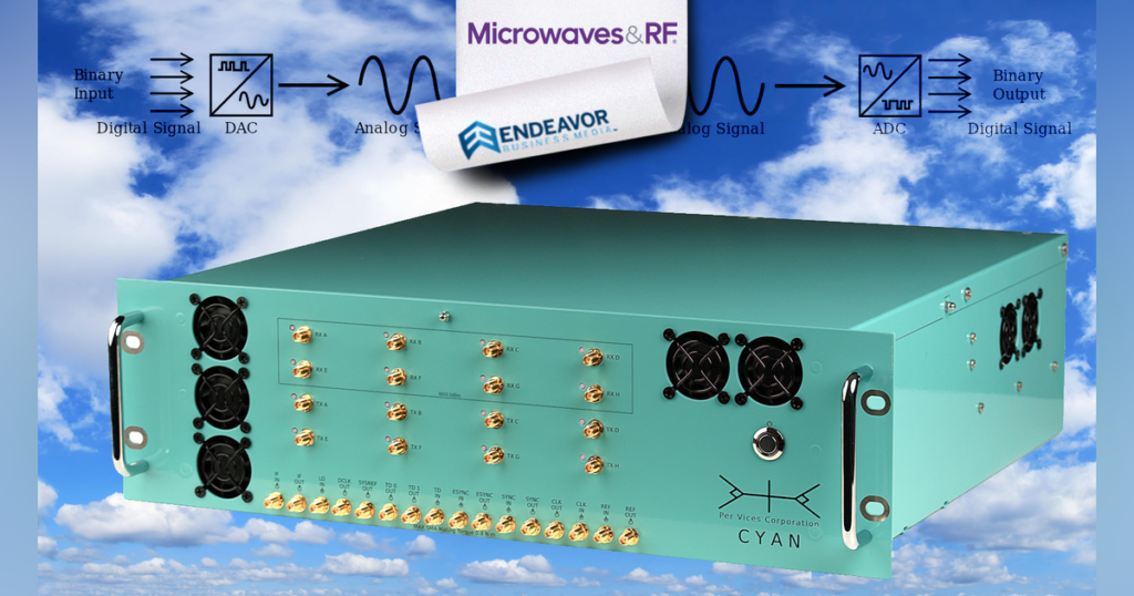
Example Application: SDR Transceivers
As a case study, we’ll discuss implementing an ADC and DAC into an SDR transceiver, an example being Per Vices’ Cyan SDR transceiver (Fig. 5). An SDR transceiver includes a radio front end and digital back end, wherein ADCs and DACs take on transmit and receive functionality. SDR mission-critical applications include spectrum monitoring and recording, radar, satellite deployment/ground station tracking, and test and measurement.
%{[ data-embed-type=”image” data-embed-id=”60ad0611a314ee613e8b48ea” data-embed-element=”span” data-embed-size=”640w” data-embed-alt=”5. Per Vices’ Cyan SDR transceiver uses ADCs/DACs to convert signals.” data-embed-src=”https://img.electronicdesign.com/files/base/ebm/electronicdesign/image/2021/05/mwrf_pv_fig5.60ad06106614b.png?auto=format&fit=max&w=1440″ data-embed-caption=”5. Per Vices’ Cyan SDR transceiver uses ADCs/DACs to convert signals.” ]}%
To achieve the high data-rate conversion and sample rates required for these applications, SDR transceivers use a pipeline ADC and interleaved DAC. Both support JESD204B serial data communicating signals decomposed into in-phase and quadrature pair (I/Q pair) components.
For an SDR application, ADCs and DACs are selected based on number of channels, sampling rate, resolution, and SFDR to meet the high-performance demands of mission-critical applications. Furthermore, SDRs used in such applications require multiple-input, multiple-output (MIMO) architectures along with a dedicated ADC/DAC in each radio chain. Such high-performance SDRs feature an analog receive chain terminating at an anti-aliasing filter and ADC with a 3-Gsample/s rate, 16-bit resolution, two input channels (for I and Q), 70.9-dB SNR, ENOB of 11.5, a 90-dB SFDR, and an operating temperature of −40 to 85°C.
On the transmit side, the DAC must be able to convert radar pulses; high-frequency modulated messages in the L, Ku, and Ka bands for satellite communications; and virtually any digital waveform to analog, before passing through an anti-imaging filter and the remaining transmit radio chain.
The DAC allows for a complex input data rate of 3 Gsamples/s per channel (I or Q data), 16-bit resolution, low SFDR and THD, low power consumption, high instantaneous bandwidth, short settling time, minimal glitch energy, and minimal temperature drift (10 ppm/°C). Because the ADC/DAC is central to the SDR’s performance, and therefore to ensuring the success of mission-critical applications, careful attention must be paid to all performance characteristics.